8085 And 8086 Microprocessor Architecture PDF BOOK KEG

The 8085 Pin Diagram has five hardware interrupt signals: RST 5.5, RST 6.5, RST 7.5, TRAP, and INTR. The microprocessor recognizes interrupt requests on these lines at the end of the current instruction execution. The INTA (Interrupt Acknowledge) signal is used to indicate that the processor has acknowledged an INTR interrupt.
Notes For You Intel's 8085 and its Architecture

Pin Diagram. This 8085 is a 40-pin microprocessor where these are categorized into seven groups. With the below 8085 microprocessor pin diagram, the functionality and purpose can be known easily. 8085 Pin Diagram Data Bus. The pins from 12 to 17 are the data bus pins which are AD 0 - AD 7, this carries the minimal considerable 8-bit data and.
8085 microprocessor IC 8085 pinouts and Working Electroinvention
The 8085 microprocessor is a 8 bit processor launched by Intel corporation in year 1976 . The 8085 microprocessor was developed using the NMOS technology . The NMOS stands for negative channel metal oxide semiconductor which is a type of technology used to manufacture IC chips. The 8085 processor is available in the market in many versions and.
8085 Microprocessor 8085 Microprocessor Architecture Gambaran

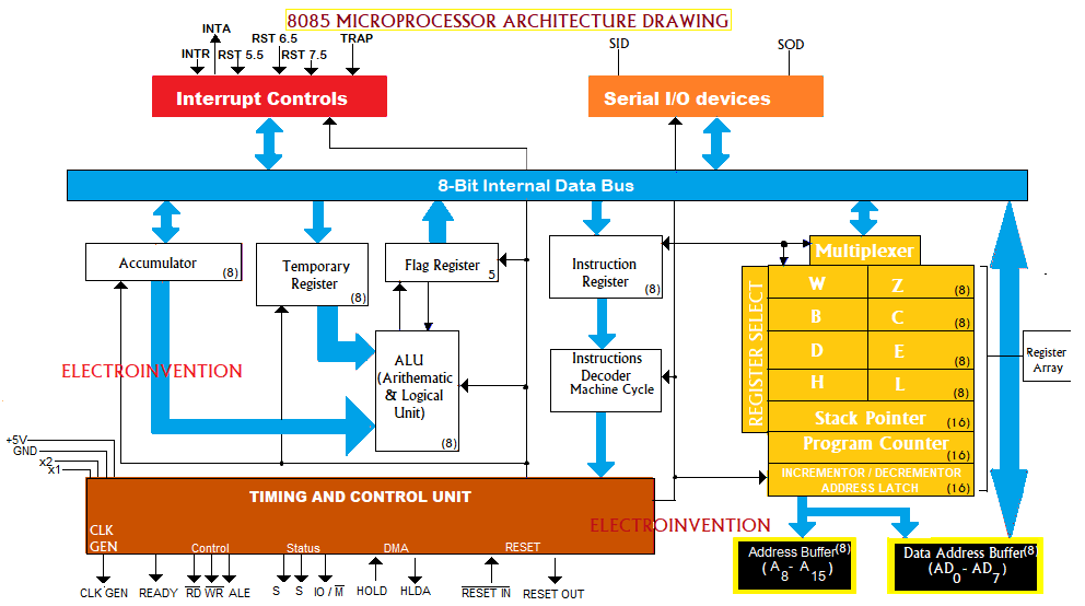
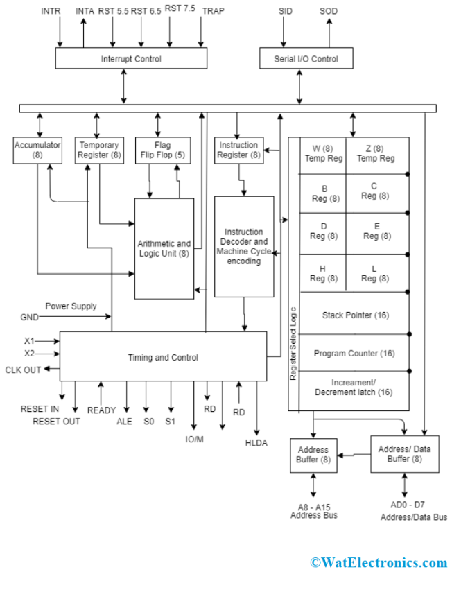
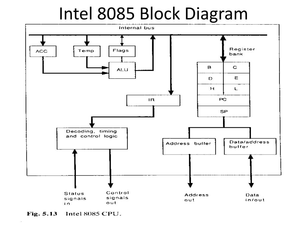
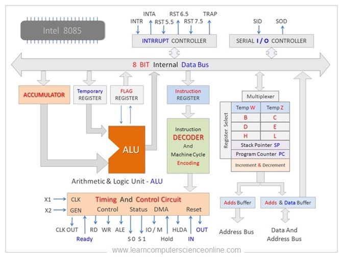
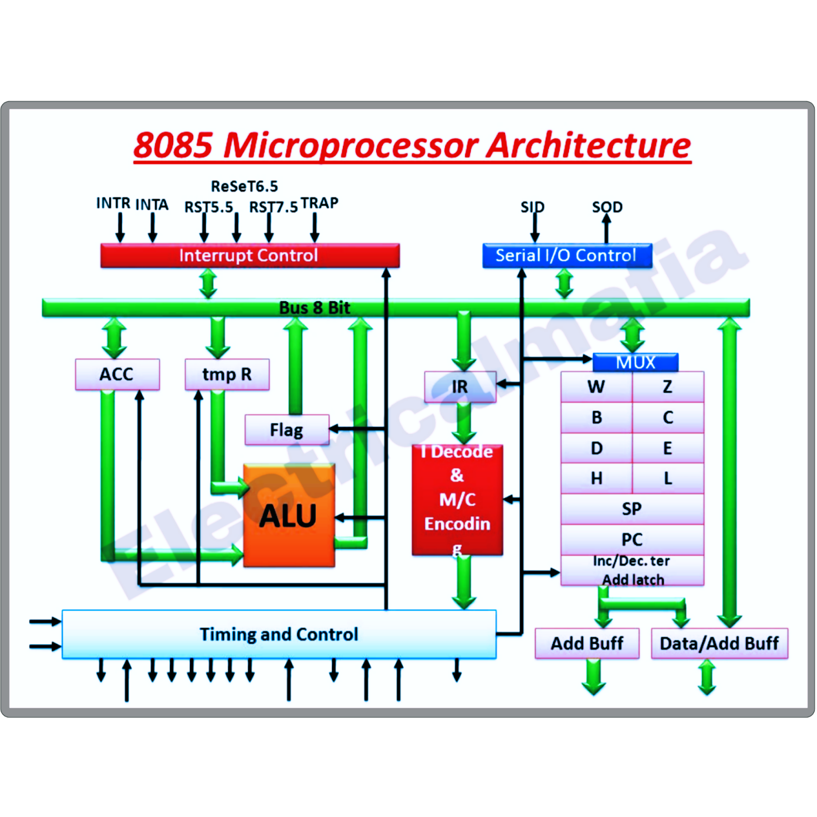
The below diagram is the internal architecture of 8085 microprocessor. This is the overview of the architecture. 8085 architecture. ALU. It is considered as a multi-operational combinational circuit that performs both logical and arithmetic operations like logical AND, logical OR, addition and subtraction. The length of the internal data bus.
The Block Diagram of 8085 Microprocessor UseMyNotes
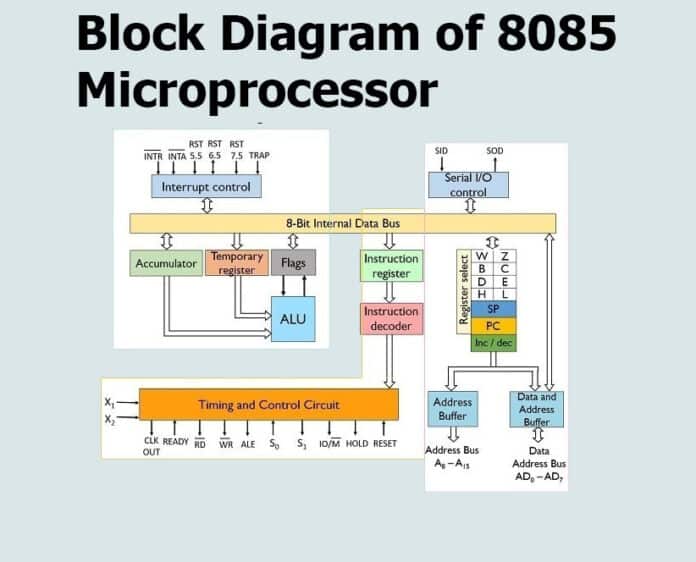
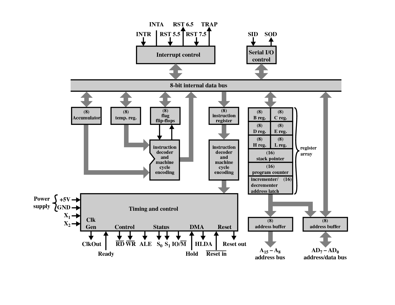
The major features of 8085 chip are 8 bit data bus, 16 bit address bus, 3.072 MHz internal clock frequency, 40 pin configuration etc. It uses +5V supply voltage for its operation. Let us understand hardware architecture of 8085 microprocessor with its internal modules with the help of 8085 block diagram and pin diagram. 8085 Architecture
Microprocessor Schematic Diagram Wiring Diagram Schemas
This playlist includes videos regarding Architecture and PIN Diagram of Microprocessor 8085. This Playlist is subpart of Microprocessor & Interfacing 8085. H.
Microprocessor 8085 Block Diagram and Architecture ETechnoG

Timing Diagram and machine cycles of 8085 Microprocessor Timing Diagram Timing Diagram is a graphical representation. It represents the execution time taken by each instruction in a graphical format. The execution time is represented in T-states. Instruction Cycle: The time required to execute an instruction is called instruction cycle.
Understanding the 8085 Architecture
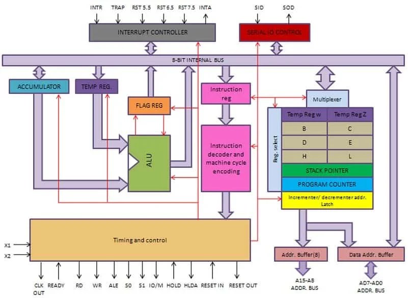
Timing and Control Unit. Synchronizes all the microoperations with the clock and generate control signals necessary for communication between microprocessor and peripherals. ← 8085 Bus Organization. 8085 Pin Diagram →. The functional block diagram or the internal architecture of the 8085 microprocessor is shown in the figure.
PPT 8085 processor PowerPoint Presentation, free download ID4551641
The 8085 microprocessor is an 8-bit microprocessor that was developed by Intel in the mid-1970s. It was widely used in the early days of personal computing and was a popular choice for hobbyists and enthusiasts due to its simplicity and ease of use. The architecture of the 8085 microprocessor consists of several key components, including the.
CSE TUBE CS2252 / CS42 / 10144 CS403 / 80250010 / EC1257 Microprocessors and Microcontrollers

Courses. Jobs. Pin diagram of 8085 microprocessor is as given below: 1. Address Bus and Data Bus: The address bus is a group of sixteen lines i.e A0-A15. The address bus is unidirectional, i.e., bits flow in one direction from the microprocessor unit to the peripheral devices and uses the high order address bus. 2.
8085 microprocessor architecture Explanation Edusera

8085 Pins - Understanding the 8085's pin diagram.. Understanding the 8085 Architecture. The architecture of any processor is the key to understanding everything about it. Its purpose, its capacity, and power, everything can be understood from a peek at the innards of the chip. Studying the 8085's internal architecture will set you up.
WORLD OF EMBEDDED Intel 8085 microprocessor & Architecture

Summary. Designed for an undergraduate course on the 8085 microprocessor, this text provides comprehensive coverage of the programming and interfacing of the 8-bit microprocessor. Written in a simple and easy-to-understand manner, this book introduces the reader to the basics and the architecture of the 8085 microprocessor.
Architechture of 8085
8085 Microprocessor Features : The features of 8085 Microprocessor include : 1.It is an 8-bit microprocessor i.e. it can accept, process, or provide 8-bit data simultaneously. 2.It operates on a single +5V power supply connected at Vcc; power supply ground is connected to Vss. 3.It operates on clock cycle with 50% duty cycle. 4.It has on.
Pin diagram of 8085 8085 Microprocessor Course
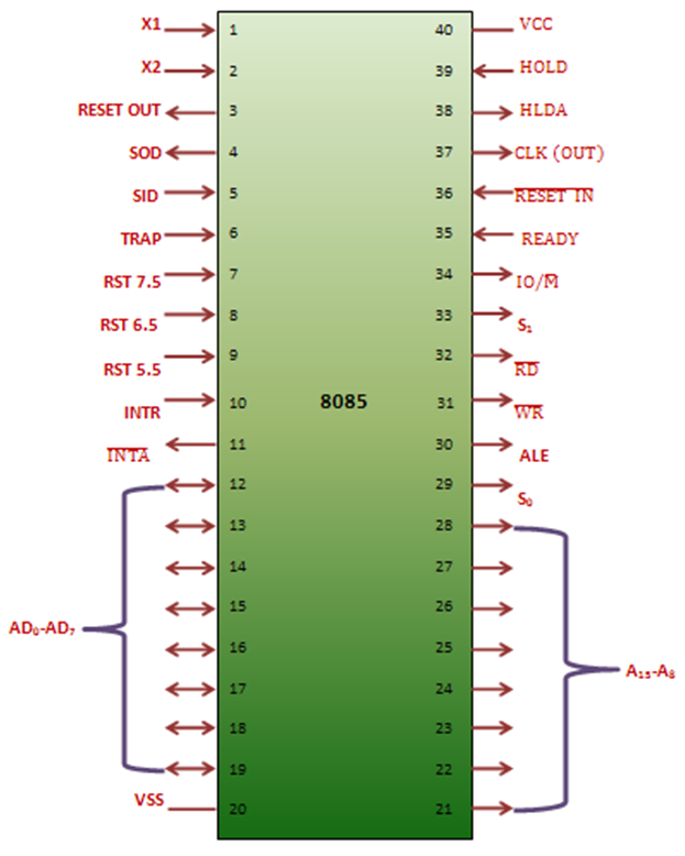
The Intel 8085 is an 8-bit microprocessor. Its data bus is 8-bit wide and therefore, 8 bits of data can be transmitted in parallel from or to the microprocessor. The Intel 8085 requires an address bus of 16-bit wide as the memory addresses are of 16-bits. The 8 most significant bits of the address are transmitted by the address bus, A-bus (pins.
8085 Architecture Intel 8085 Microprocessor Architecture Block Diagram
Block Diagram & Architecture Of 8085 Microprocessor Watch More Videos at: https://www.tutorialspoint.com/videotutorials/index.htmLecture By: Gowthami Swarna,.
Architecture of 8085 microprocessor ElectricalMafia
Microprocessor - 8085 Architecture. 8085 is pronounced as "eighty-eighty-five" microprocessor. It is an 8-bit microprocessor designed by Intel in 1977 using NMOS technology. It has the following configuration −. 8-bit data bus. 16-bit address bus, which can address upto 64KB. A 16-bit program counter.